Our R&D Expertise

Explore the technology areas where Singapore has built deep capability, from early-stage research through to platforms ready for industry.

As the demand for computing performance grows, tighter integration of processors, memory, photonic ICs and other specialised ICs becomes increasingly important. Advanced packaging enables this heterogeneous integration, creating compact, energy-efficient and high-performance systems.

Built on More Than Two Decades of Advanced Packaging R&D

Singapore’s advanced packaging capabilities have been built over more than two decades, evolving alongside the growing needs of semiconductor systems. Today, we offer a broad portfolio including 2.5D and 3D integration, flexible and rigid hybrid integration and thermal management.

These capabilities support the integration of logic, memory, photonics, RF, sensing and power technologies. Through system technology co-optimisation (STCO) and package and system co-design, Singapore brings together electrical, mechanical, RF and thermal modelling; process development; failure analysis; and functional and reliability testing to develop and evaluate advanced packaging solutions.

Our Public R&D Performers

Agency for Science, Technology and Research (A*STAR)

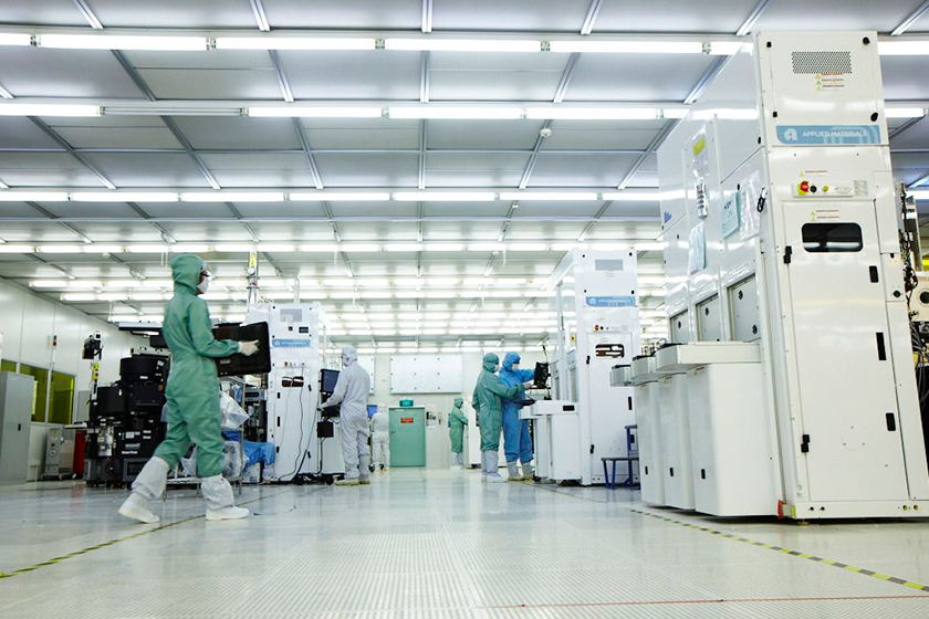
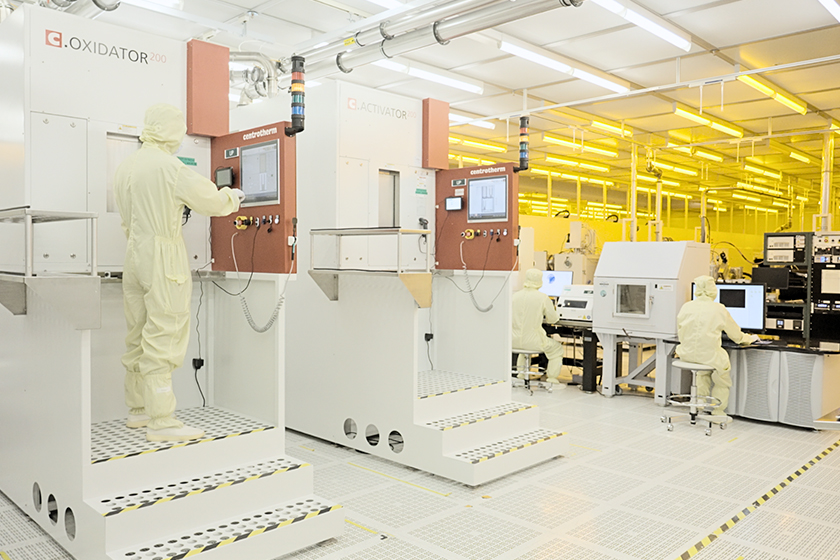
A*STAR focuses on technology development and translational R&D in advanced packaging, supported by industry-grade 200 mm and 300 mm tools. Its capabilities span 2.5D and 3D integration, high heat flux chip coolers and cryogenic chip packaging. A*STAR’s advanced packaging development lines support wafer-level process development, R&D pilot runs, small-volume production and technology transfer, providing companies with a pathway to de-risk new packaging technologies towards manufacturing.

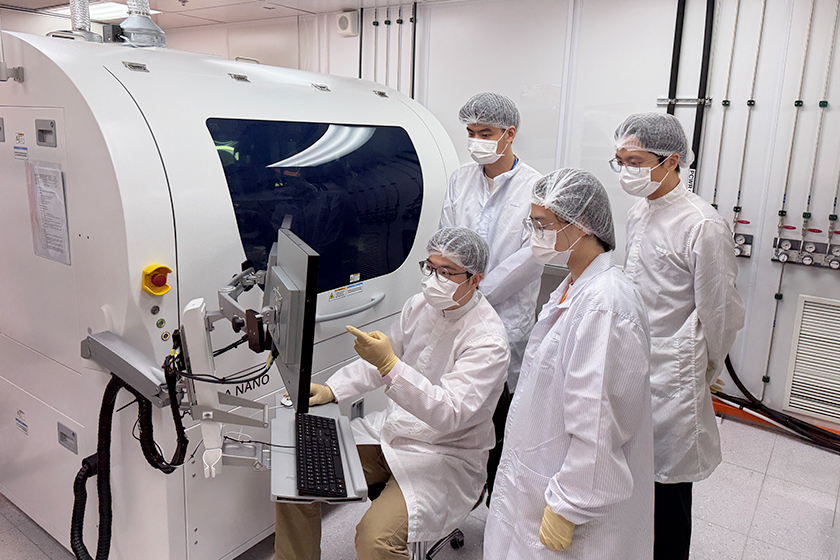
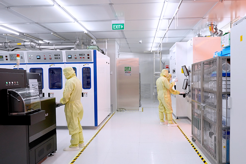
A*STAR’s 200 mm and 300 mm advanced packaging lines at the Applied Materials–A*STAR Advanced Packaging Joint Lab
National University of Singapore (NUS)

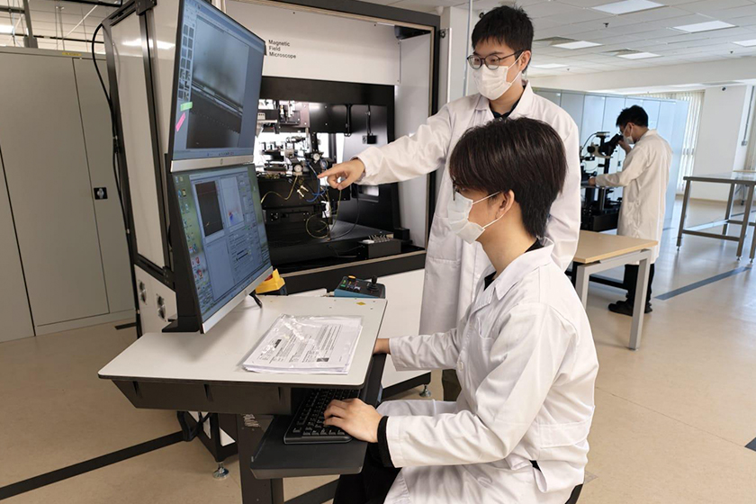
NUS’ Singapore Hybrid-Integrated Next-Generation μ-Electronics (SHINE) Centre focuses on pathfinding in heterogeneous and hybrid integration using high-precision die bonding and additive manufacturing. It develops proof-of-concept systems combining diverse dies, materials and substrates beyond conventional wafer-level packaging. Its capabilities support electronic and photonic IC integration, flexible hybrid electronics, wearable sensors and non-destructive 3D magnetic-field imaging for defect localisation in 2.5D and 3D packages.

NUS SHINE’s Magnetic Field Imaging (MFI) system for fault localisation in advanced semiconductor packages

Our Industry Collaborators

Large AI models require massive amounts of data to be exchanged among processors, memory and servers. As AI systems continue to scale, the speed of data movement and the energy it consumes are limiting overall system performance. One solution is to move data with photons instead of electrons. Optical transceivers are already widely deployed for long-distance communications between countries, cities and buildings. Within a data centre, silicon photonics-based optical transceivers are increasingly replacing conventional electrical links between racks and between servers. Ongoing R&D aims to enable optical connectivity between processors and memory, supporting the next generation of high-performance AI computing.

From Device Innovation to Wafer-Scale Integration for Ultra-High-Speed Optical Connectivity

Singapore has invested in silicon photonics R&D since 2006, building capabilities in photonic device and circuit design, materials development, heterogeneous integration, wafer fabrication, prototyping and chip-scale to wafer-scale electro-optical testing and characterisation.

We offer a Silicon Photonics Heterogeneous Integration (Si-PHI) platform that uses industry-standard die-to-wafer bonding and CMOS-compatible wafer-scale fabrication to integrate best-in-class materials onto a photonics chip. The platform combines silicon (Si) and silicon nitride (SiN) for optical routing, germanium (Ge) for photodetection, thin-film lithium niobate (TFLN) for ultra-high-speed modulation and indium phosphide (InP) for light generation and amplification. This approach enables compact, high-performance and manufacturable optical transceivers, with demonstrated optical data transmission at 400 Gbps per lane and beyond.

Our Public R&D Performers

National Semiconductor Translation and Innovation Centre (Advanced Photonics)

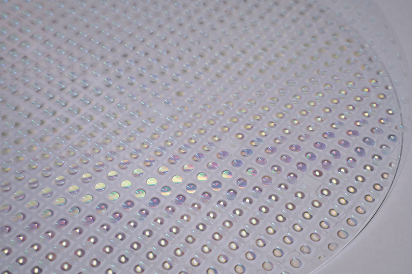
NSTIC (Advanced Photonics) is Singapore’s national platform for photonics technology development and translation, focusing on silicon photonics and flat optics. For silicon photonics, its end-to-end capabilities span 200 mm and 300 mm wafer-level process development and fabrication, three integration platforms comprising SiN-on-SOI, TFLN-on-Insulator and PHI TFLN-on-SiPh, together with electro-optical testing. Companies can access these capabilities through multi-project wafer (MPW) services and dedicated R&D runs to develop and prototype application-specific photonic integrated circuits (PICs), helping to accelerate innovation and commercialisation.

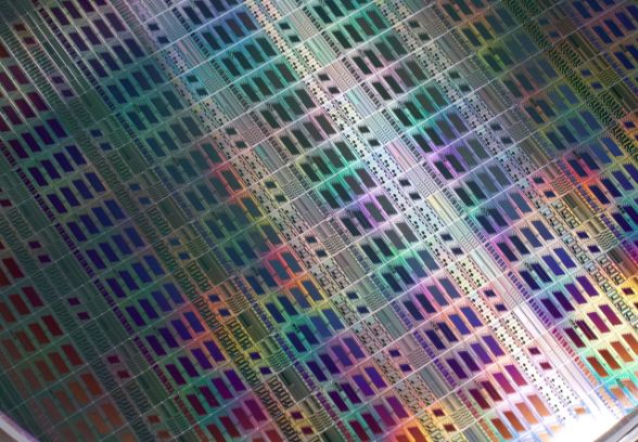
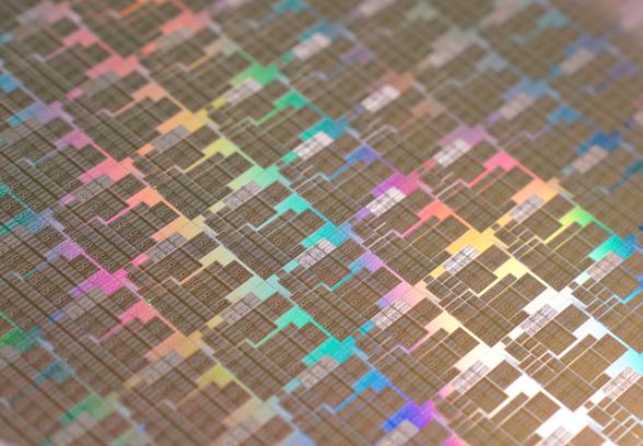
NSTIC (Advanced Photonics) 200 mm PHI wafer, integrating TFLN on SiN through die-to-wafer bonding
Nanyang Technological University (NTU)

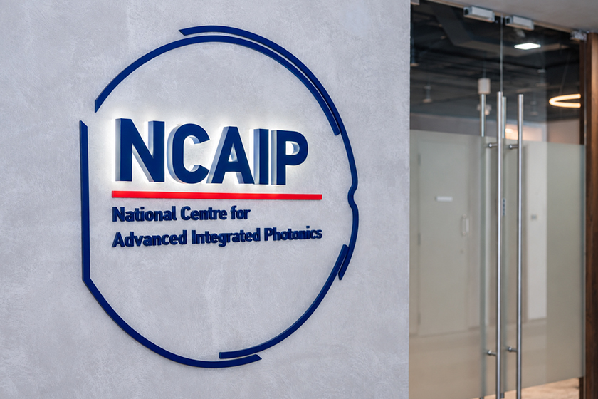
The National Centre for Advanced Integrated Photonics (NCAIP) conducts research into next-generation silicon photonics integrated circuits, including wafer-scale heterogeneous integration of III-V lasers and photodetectors, high-speed electro-optic modulators and low-loss waveguide platforms, predominantly for data communication in AI data centres. NCAIP also explores emerging photonic materials and devices for quantum, MWIR and THz applications, aiming to provide sensing, data transmission and spectroscopy solutions.

NTU’s National Centre for Advanced Integrated Photonics
National University of Singapore (NUS)

NUS’ Singapore Hybrid-Integrated Next-Generation μ-Electronics (SHINE) Centre conducts research into high-performance photonic devices by combining silicon photonics with lithium niobate, ferroelectrics, oxide semiconductors and 2D materials. Its work includes programmable wavelength division multiplexing (WDM) photonic memory and heterogeneous integration of thin-film lithium niobate (TFLN) on silicon photonics wafer via micro-transfer printing.

NUS SHINE’s Micro-Transfer Printing (MTP) system for heterogeneous integration of photonic and electronic chiplets
Singapore University of Technology and Design (SUTD)

SUTD’s Photonics Devices and Systems Group conducts research in silicon photonics, photonic integrated circuits and nonlinear photonics. Its work spans micro-resonator frequency combs, high-performance photonic devices, optical signal processing, high-speed communications as well as emerging topics such as topological photonic devices and 3D-printed photonic structures. The group also investigates fundamental and applied nonlinear phenomena, such as frequency conversion, parametric amplification, ultra-fast optical dynamics, optical solitons and supercontinuum generation.

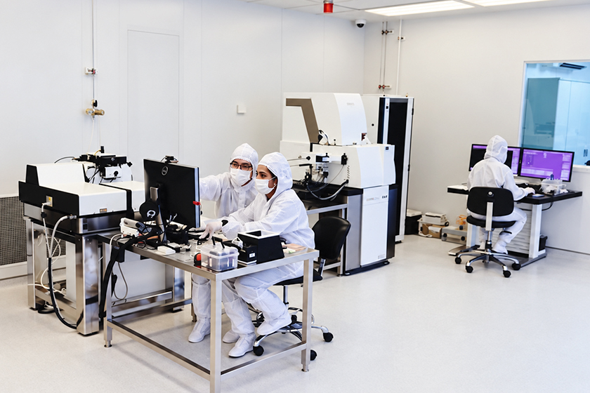
SUTD’s cleanroom nanofabrication facility supporting research in integrated photonic devices

Our Industry Collaborators

Piezoelectric micro-electro-mechanical systems, or piezoMEMS, convert electrical energy into mechanical movement and vice versa. R&D in thin-film piezoMEMS devices using wafer-level processes is becoming increasingly important because traditional piezoelectric sensors and actuators that are made from bulk crystals struggle to meet the growing demand for higher performance, miniaturisation, lower cost and lower power consumption.

Accelerating the Path from Prototyping to Production

Singapore has expertise in the design, development and wafer fabrication of thin-film lead zirconate titanate (PZT) and scandium aluminum nitride (ScAlN) piezoMEMS devices. To shorten the path from research to production and reduce technology transfer risk, we offer “Lab-in-Fab” in addition to conventional “Lab-to-Fab” services on our 200 mm line. The Lab-in-Fab, established in partnership with A*STAR, STMicroelectronics and ULVAC in 2020, enables R&D to take place within a high-volume manufacturing environment, allowing manufacturability to be considered earlier in development.

Our Public R&D Performers

Agency for Science, Technology and Research (A*STAR)

A*STAR focuses on technology development and translational R&D for piezoMEMS, supported by its 200 mm Lab-in-Fab and Lab-to-Fab services. Its capabilities span materials development, device and system design and modelling, wafer-level process development, prototyping through multi-project wafer (MPW) and dedicated runs, characterisation, packaging and technology transfer for volume production. The materials offered include sol-gel PZT, PVD PZT and ScAlN, supporting piezoMEMS devices for applications such as medical imaging, range finding, RF communications and timing.

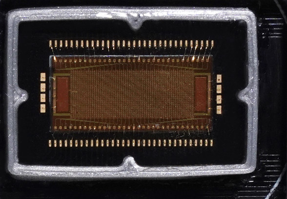
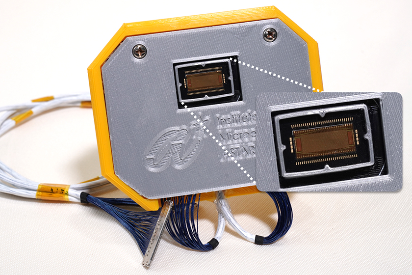
PZT-based 64-channel PMUT array prototype for medical imaging, jointly developed by A*STAR and STMicroelectronics through the Lab-in-Fab
National University of Singapore (NUS)

NUS conducts research across a broad range of MEMS technologies, including optical, THz, piezoelectric and power MEMS. Within piezoMEMS, its work focuses mainly on device design and system demonstration, investigating barium titanate (BTO) and sodium niobate (NNO) for RF filters and gas sensors, polyvinylidene fluoride (PVDF) films and nanofibres for wearable sensors and thick-PZT bimorph microcantilevers for sensing and energy harvesting.

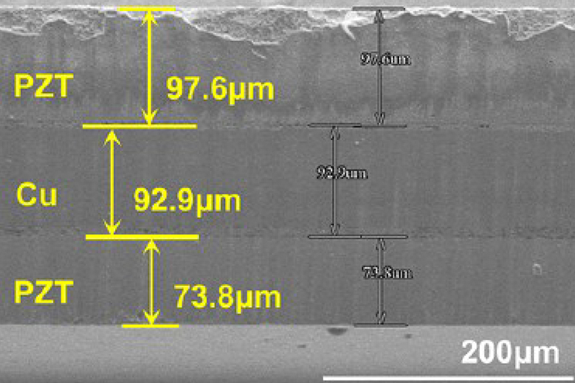
Cross-sectional SEM image of a thick-PZT bimorph microcantilever developed by NUS for sensing and energy-harvesting applications
Nanyang Technological University (NTU)

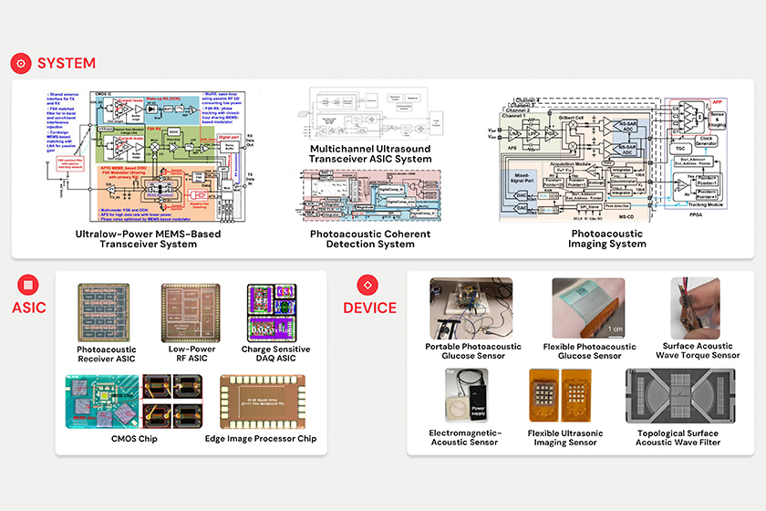
NTU conducts piezoMEMS research focused on the design of integrated circuits, devices and complete systems for piezoMEMS applications, particularly in ultra-low-power wireless communication, ultrasonic imaging and photoacoustic sensing. Its work covers circuit/device-level and system-level capabilities, including low-power RF and ultrasound transceiver ASICs, multichannel data-acquisition and edge-processing circuits, flexible ultrasonic sensors, surface acoustic wave devices and portable photoacoustic sensing platforms.

Examples of NTU’s piezoMEMS research across integrated systems, ASICs and sensing devices

Our Industry and Research Collaborators

Conventional optical systems rely on multi-element refractive lenses that are bulky and require precise alignment. Achieving this alignment can make lens assembly more complex and costly, while integrating conventional optics with semiconductor devices can also be challenging due to differences in size and materials. Flat optics addresses these limitations by using nanoscale structures to control light within ultra-thin surfaces, enabling compact, lightweight, multifunctional and semiconductor-compatible optical systems. This opens new opportunities for AR/VR, imaging, sensing, displays and next-generation consumer and semiconductor applications.

From Design to Wafer-Scale Fabrication and Integrated Systems

Building on more than a decade of R&D in flat optics since 2010, Singapore has developed capabilities in optical design and device simulation, wafer-scale manufacturing, optical characterisation and device integration. This end-to-end capability enables innovative flat-optics concepts to be translated from design to fabricated devices and functional prototypes, while ensuring that the resulting devices meet performance specifications and are manufacturable with good yield and repeatability. We enable companies to accelerate flat-optics product development from concept to product-ready solutions.

Our Public R&D Performers

National Semiconductor Translation and Innovation Centre (NSTIC)

NSTIC is Singapore’s national platform for photonics technology development and translation, focusing on silicon photonics and flat optics. For flat optics, the platforms offered are 300 mm amorphous silicon metasurface on silicon and glass wafers, 300 mm silicon nitride metasurface on glass wafers and 300 mm titanium dioxide metasurface on glass wafers, with advanced capabilities in three-layer and double-sided amorphous silicon metasurfaces on glass.

NSTIC’s TiO₂-on-glass metalens fabricated on a 300 mm wafer platform

Our Industry Collaborators

Power electronics converts and controls electrical energy so that it can be delivered efficiently at the voltage, current and frequency required by electrical and electronic systems. While silicon remains widely used in low-voltage (< 600 V) power electronics, advances in wide-bandgap semiconductors such as silicon carbide (SiC) and gallium nitride (GaN) are extending the performance range of power devices. SiC supports efficient high-voltage and high-power operation with greater thermal capability, while GaN enables efficient, compact power conversion at low to medium voltages.

Advancing Power Devices from Design to Manufacturing

Singapore offers expertise in the design and modelling, process development, wafer fabrication, device prototyping, characterisation, reliability and system-level design of power semiconductors. Our capabilities are centred on SiC power devices such as trench, planar and super-junction MOSFETs as well as diodes, alongside early-stage research into vertical GaN power devices. Equipped with industry-grade tools, our 200 mm line enables equipment and materials suppliers, device companies and manufacturers to partner with us in developing process flows and devices, with commercial manufacturability considered from the outset.

Our Public R&D Performers

National Semiconductor Translation and Innovation Centre (Power Electronics)

NSTIC (Power Electronics) is Singapore’s national platform for wide-bandgap power semiconductor technology development and translation. It operates a 200 mm SiC line that supports wafer-level process development and device prototyping for SiC planar, trench and super-junction MOSFETs and diodes. Its capabilities also include power module packaging and wafer- and package-level characterisation and reliability testing, spanning static, dynamic, cryogenic and high-voltage measurements up to 10 kV.

200 mm SiC line at NSTIC (Power Electronics) for wafer-level process development and device prototyping
National University of Singapore (NUS)

NUS conducts research at both device and system levels in power electronics. At the device level, its work covers device physics and modelling, with a focus on the design, simulation and experimental demonstration of high-voltage and wide-bandgap power semiconductor devices, including GaN power devices and other advanced device structures. At the system level, its work spans power electronics design and real-time simulation of systems at kilovolt and megawatt scales, as well as power converter and system hardware development and testing up to 1.7 kV, 22 kW and 200 °C. This includes high-frequency power electronics, control and their supporting components.

NUS-developed power electronics hardware under laboratory testing for EV battery charging, with AC-to-DC and DC-to-DC conversion for grid and solar power inputs
Singapore Institute of Technology (SIT)

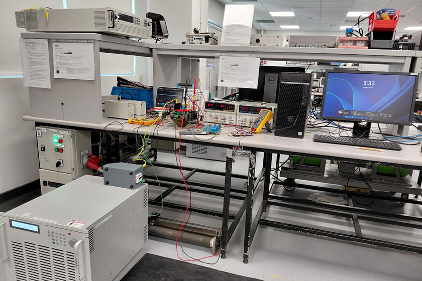
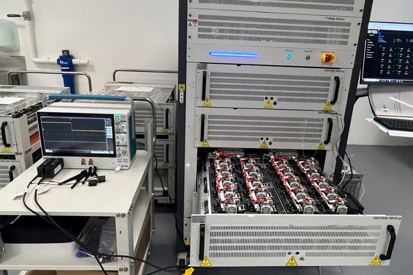
SIT focuses on power semiconductor characterisation and reliability testing, as well as system-level power electronics design, integration and validation. Its in-house high-voltage semiconductor testing facilities, including an HTDRB tester, support automotive-standard testing at voltages up to 1.2 kV, voltage slew rates up to 50 V/ns and temperatures up to 150 °C. These facilities also support accelerated lifetime testing, power cycling, failure analysis and thermal monitoring. At the system level, its work spans power converters, motor drives, battery energy management, thermal management, digital control, electromagnetic interference (EMI) and electromagnetic compatibility (EMC), and hardware-in-the-loop (HIL) validation.

SIT’s in-house HTDRB test setup for power semiconductor reliability testing to automotive standards

Our Industry Collaborators

Radio frequency (RF) communications enable devices to communicate with one another without wires. The laws of physics dictate that higher frequencies are needed to transmit wirelessly at higher data rates. R&D in RF gallium nitride (RF GaN) is important because it addresses the limitations of current materials such as gallium arsenide (GaAs), silicon germanium (SiGe) and silicon, which are unable to simultaneously operate at high frequencies, high power and high energy efficiency.

Developing RF GaN Technologies for Performance and Scale

Singapore has expertise in the design and modelling of GaN high electron mobility transistors (HEMTs), design of monolithic microwave ICs (MMICs), epitaxial growth of III-nitrides HEMT heterostructures on silicon (Si) and silicon carbide (SiC) substrates, process development, wafer fabrication of GaN-on-SiC and GaN-on-Si devices, characterisation and reliability testing. We offer a 150 mm GaN-on-SiC technology platform for applications requiring high-frequency operation and high output power, alongside a 200 mm GaN-on-Si platform that supports CMOS-compatible processing and greater manufacturing scalability.

Our Public R&D Performers

National Semiconductor Translation and Innovation Centre (GaN)

NSTIC (GaN) is Singapore’s national platform for GaN technology development and translation, supporting R&D from proof-of-concept and prototyping through to small-volume manufacturing. It provides boutique foundry services for 150 mm GaN-on-SiC and 200 mm GaN-on-Si wafer processing, electrical testing and reliability testing. Its first process design kit (PDK) for 0.25 µm GaN-on-SiC is expected to be ready by Q1 2027, followed by a second PDK for GaN-on-Si in Q2 2027. NSTIC (GaN) also operates an electrical test lab for continuous wave or pulsed-based RF scattering parameter up to 65 GHz and a reliability test lab for DC and RF high-temperature operating life (HTOL) testing.

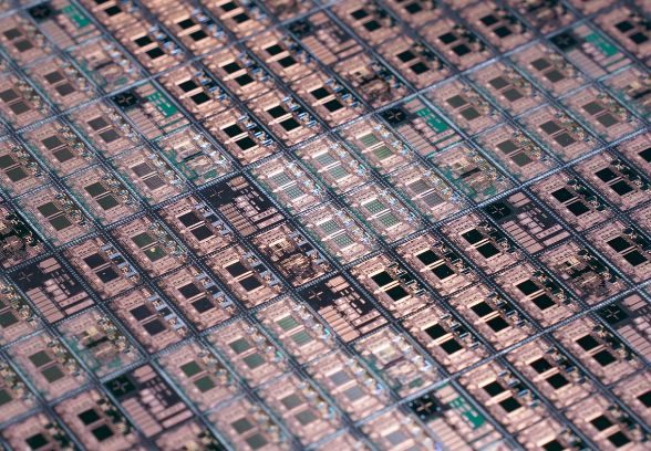
150 mm GaN-on-SiC and 200 mm GaN-on-Si line at NSTIC (GaN)

Our Industry Collaborators

Computing, wired communications and wireless communications are central to modern electronic systems. As these systems advance, integrated circuits (ICs) must perform under extreme conditions. These include harsh environments, such as operating in space for satellites or at cryogenic temperatures for quantum computing, as well as the need to achieve extreme performance, such as 400 Gbps per lambda and higher speeds for optical communications and millimetre wave (mmWave) frequencies for 6G wireless communications.

Designing Radiation-Hardened, mmWave and Cryogenic Chips

Singapore offers expertise in designing radiation-hardened, mmWave and cryogenic chips. Our capabilities span transistor modelling, circuit design and simulation, wafer fabrication processes, advanced packaging and testing. These enable us to accurately translate system-level requirements into optimised circuit architectures, select the most suitable semiconductor processes, design, fabricate and package the chips, and validate their performance.

Our Public R&D Performers

Agency for Science, Technology and Research (A*STAR)

A*STAR focuses on technology development and translational R&D of ICs for extreme operating conditions and performance requirements, taking IC designs from simulation through chip fabrication, testing and validation. Its strengths span radiation-hardened RISC-V compute cores, mmWave beamforming ICs (BFICs) and RF power amplifiers (PAs) as well as low-power cryogenic ICs for control and readout. A*STAR also offers the EDA Garage programme, which gives local startups and SMEs access to pay-per-use EDA software licences.

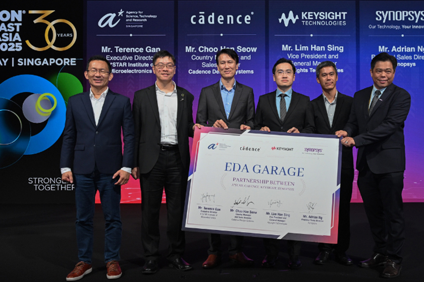
A*STAR’s EDA Garage programme, launched in 2025 in collaboration with Cadence, Keysight and Synopsys

Our Industry Collaborators

Let us help you find the right team to drive your next breakthrough.